Видео: Pcb
Подборка новых видео на тему Pcb на сегодня 18 April 2026 года
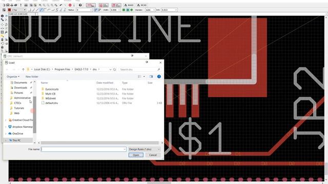
Яндекс Дзен Компьютерное SHOW Канал Компьютерные Ошибки Стандарт PCI Express является одной из основ современных компьютеров. Слоты PCI Express уже давно занимают прочное место на любой материнской плате декстопного компьютера, вытесняя другие стандарты, например, такие как PCI. Но даже стандарт PCI Express имеет свои разновидности и отличающийся друг от друга характер подключения. На новых материнских платах, начиная примерно с 2010 года, можно увидеть на одной материнской плате целую россыпь портов, обозначенных как PCIE или PCI-E, которые могут отличаться по количеству линий: одной x1 или нескольких x2, x4, x8, x12, x16 и x32. Давайте с вами выясним почему такая путаница среди казалось бы простого периферийного порта PCI Express.... Смотреть видео...
hellow friends, This is video about, PCB Design Sinhala | How to design pcb using proteus | PCB design tutorial This video include, in this video I talk about how to make pcb design using proteus software.i hope you can inprove your pcb design knowledge through this video. Proteus crack version- My videos, PCB design Without laser printer- PCB design sinhala tutorial- Make mINI Hand drill at home- Make adjustable power supply At Home_ LM 317T voltage regulator - How to make fire alarm system- Rotate direction change using by l298N motor driver- Automatic hand sanitizer dispenser- Solar Power Bank |How To make Solar Powered power bank- How To Make Distance Meter using Arduino | Ultrasonic sensor project- LED chaser... Смотреть видео...
🧧 Чат с сообществом: 👀 Telegram (канал): 🎲 Аналитический сервис: созданный 👁GURU.Markets👁 Претензии, вопросы, сотрудничество, и другое пишите сюда: ⌨️ Telegram: 💬 WhatsApp: ✉️ Email: help@guru.markets ⌚ Тайм коды: 00:00 - Вступление проекта, общие сведения по обзору компании PCB BANCORP. (PCB) 01:30 - Оценка рыночной и балансовой капитализации организации PCB Bancorp (PCB) 02:57 - Оценка долговых обязательств компании PCB Bancorp (PCB) 03:17 - Оценка P/E - Forward Price-to-Earnings PCB Bancorp (PCB) (PCB) 04:10 - Анализ P/S - Forward Price-to-Sales PCB BANCORP (PCB) 05:23 - Анализ прибыльности продаж компании PCB Bancorp (PCB) 05:49 - Обзор занимаемой доли по числу работников организации PCB BANCORP. (PCB) в подкатегории 06:46 -... Смотреть видео...
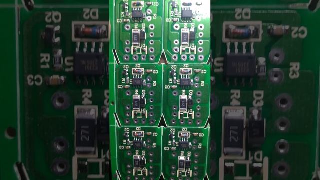
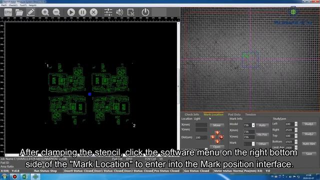
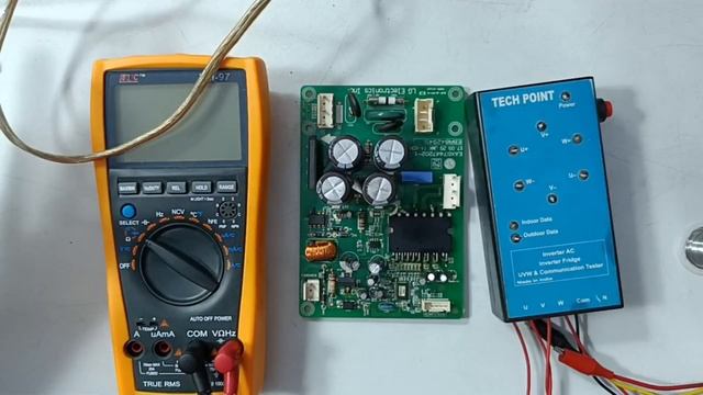
PCB Visual And Touchup Process #PCB विजुअल और टचअप प्रोसेस, दुनिया का कोई भी SMD PCB और असेंबल PCB विजुअल करने का आसान तरीका#pcb #smd #pcbassembly #PCB visual#smtechnical soldering dry soldering Smt machine SMT Programming SMT Process SMT Soldering Process SMT Components SMT Components Identifications SMT components polarity smt components resistors smt resistor value reading smt capacitors smt ic smt diode smt chip resistor SMD Components SMD Components Identifications SMD components polarity SMD components resistors SMD resistor value reading SMD capacitors SMD ic SMD diode SMD chip resistor smd Color code solder paste solder past printing process oven profiling oven soldering oven temperature profiling oven pcb soldering oven soldering... Смотреть видео...
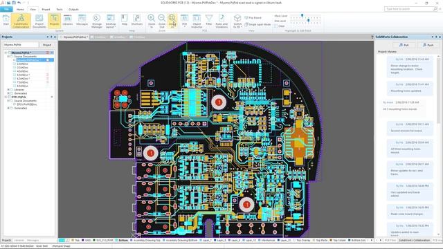
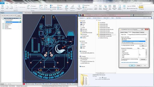
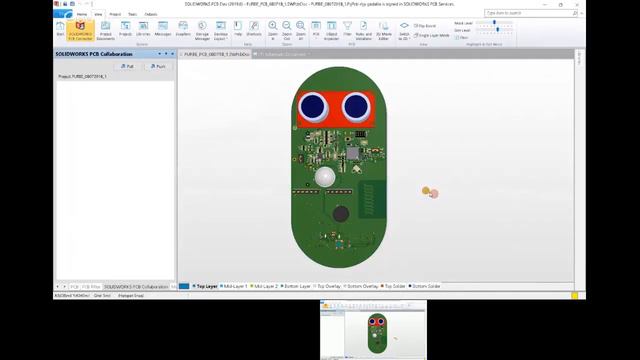
In part two of learning SOLIDWORKS PCB we look at how to use PCB Services Solid Solutions is the leading SOLIDWORKS services provider delivering an expansive portfolio of solutions, ranging from 3D design (CAD), manufacturing (CAM) and data management (PDM/PLM) software tools, training, and technical support services, through to comprehensive business transformation programmes. Solid Solutions supports a community of more than 15,000 UK and Ireland-based customers, who encompass product designers, mechanical engineers, designers, manufacturers, and educational institutions across a wide range of industries. Need to find out more? Whether you're wondering where to start, looking to pick up some new tricks, or are just curious about... Смотреть видео...
Get ten 100x100mm one or two layer high quality PCBs for just $5 plus shipping from sponsor of this video: My demonstration on how to reverse-engineer simple PCB with KiCAD7. 0:00 Example target 0:25 Sponsored by PCBWAY.COM 1:11 Steps before KiCAD 1:30 KiCAD First steps 2:50 Importing photos 4:20 Placing components 6:05 Rest of the process I removed components one by one from sacrificial module and measured them. Then I added those parts to KiCAD schematic editor, with same reference numbers as on the actual PCB. Next I sanded solder mask off from the PCB, took photos of both sides. I flipped the backside to make it align with photo of the front side. Photos were cropped to exact PCB size, to make it easier to scale them in... Смотреть видео...
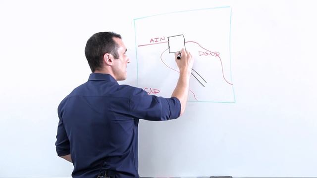
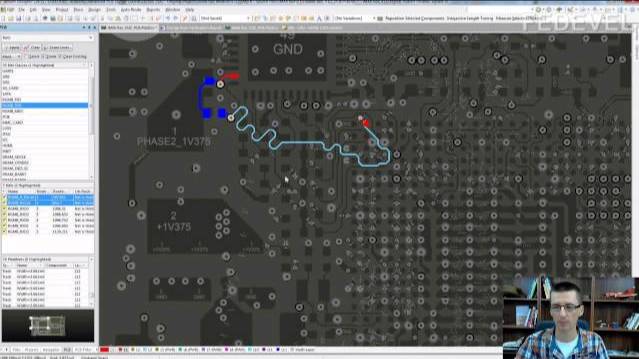
Tech Consultant Zach Peterson explores the different types of ground PCB designers might come across in schematics, datasheets, reference designs, etc. He dives deep into PGND, AGND, DGND, SGND, and more so you can learn how to have a consistent ground potential in the midst of all the varying connections. 0:00 Intro 0:48 DGND, AGND, SGND, & PGND 4:16 Analog-to-Digital Converter (ADC) Example 8:00 PCB Layout Example 10:29 Net Tie Location? 12:33 Power Converters For more PCB Layout videos, click here: For more PCB Design for Intermediate Users videos, click here: For more Tech Consultant Zach Peterson videos, click here: ? Should You Use Star Grounding for Analog and Digital Ground Separation?: ? Create a Buck-Boost Power... Смотреть видео...
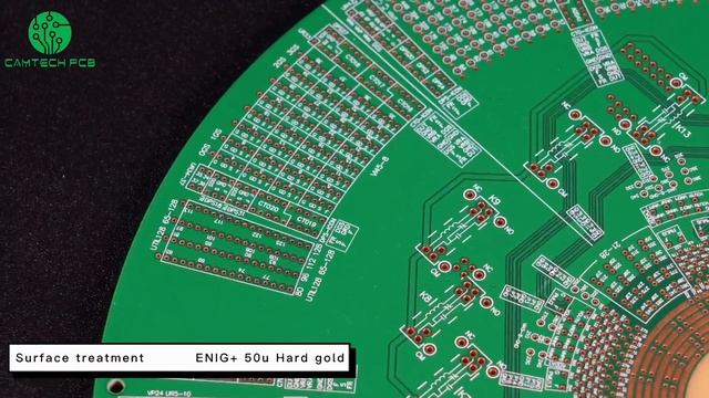
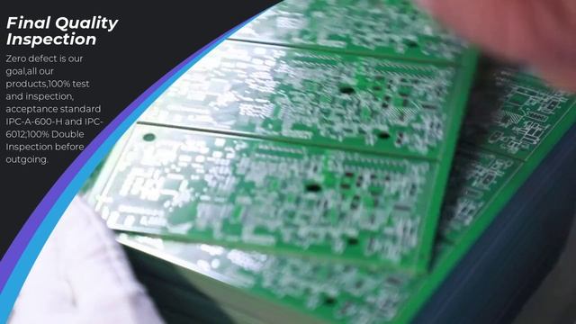
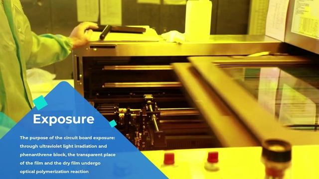
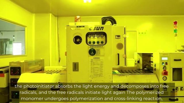
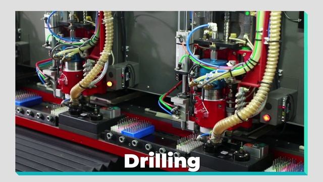
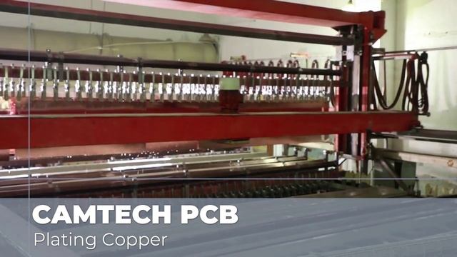
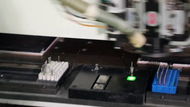
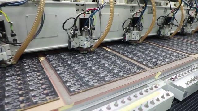
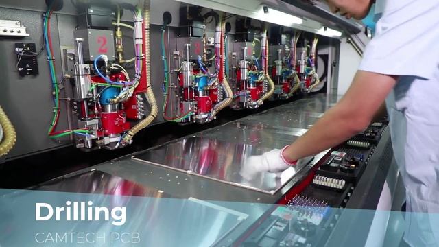
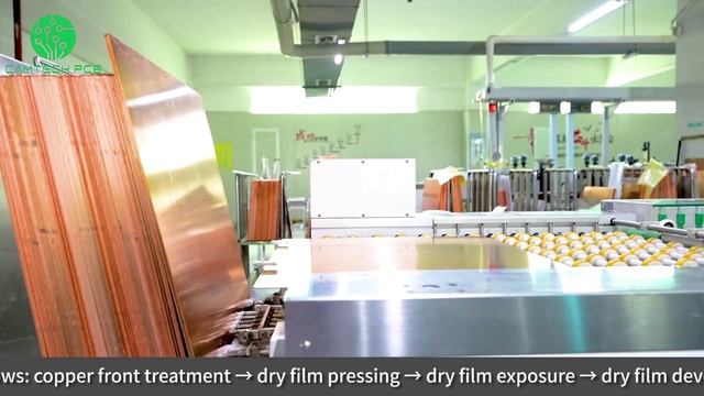
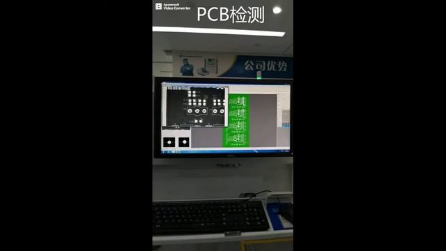
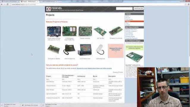
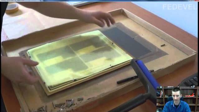
Watch how PCB is manufactured and how boards are assembled. Thank you very much to JLC for helping me to create this video. - JLCPCB 1-8 Layers for $2: - FEDEVEL online courses: Chapters: 00:00 What is this video about 00:14 Raw material cut to panels 01:21 Cleaning PCB 02:59 Photosensitive film applied (Building layers L2 & L3) 03:56 Exposing L2, L3 05:39 Developing L2, L3 06:36 Etching L2, L3 07:27 Removing photosensitive layer 08:01 AOI - Automated Optical Inspection 08:55 Making copper rougher 10:43 Adding prepreg 11:19 Adding copper sheets - Top and Bottom layer (L1, L4) 13:01 Baking PCBs, oven room 14:54 Splitting to two panels again 17:06 Adding aluminum sheet 17:30 Drilling 19:39 Plating 20:52 Electroless plating 24:18... Смотреть видео...
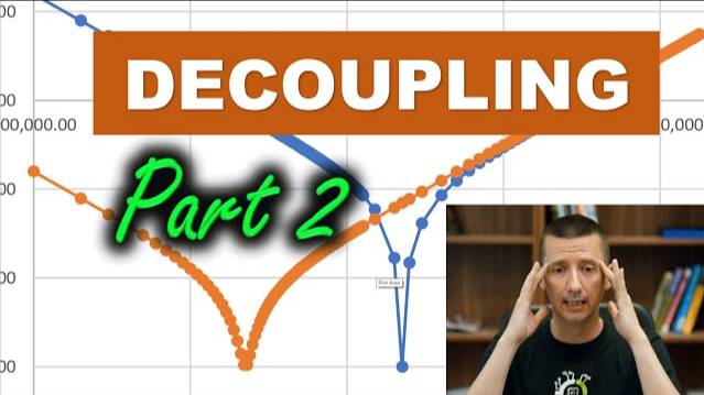
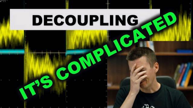
When capacitor is an inductor ... Part 1: PCB Layout & Decoupling - Explained why it's so complicated Part 2: PCB Layout & Decoupling - Understanding Impedance Part 3: PCB Layout & Decoupling - Measuring and Fixing Links: - PCB Layout & Decoupling - Explained why it's so complicated (Part 1): - Calculating Impedance Webpage: - Series Resonance in RLC Circuit: ------------------------------------------------------ Would you like to support me in what I do? It's simple: - you will help me a LOT, when you sign up for one of our Schematic and PCB Design online courses at The other ways to support me in what I do are: - Subscribe to this channel - support me through Patreon page - sign up for my Udemy course, Learn to Design Your... Смотреть видео...
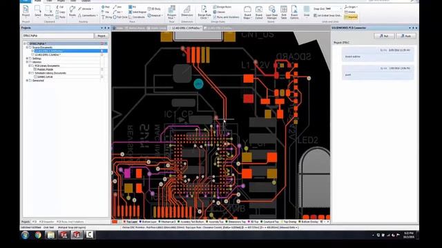
The video will show you how to install the SOLIDWORKS PCB Connector as an Altium Designer Extension. NOTES: 1. Prior to installing the SOLIDWORKS PCB Connector, the following must be installed: • Altium Designer • SOLIDWORKS PCB Services -or- Altium Vault (if AD17 or prior) or Nexus (if AD18 or later) • SOLIDWORKS SOLIDWORKS PCB Services does not require a license. This must be installed prior to the installation of the SOLIDWORKS PCB Connector. This installation is separate from SOLIDWORKS and Altium Designer. If the SOLIDWORKS PCB Connector will be installed on more than one computer, SOLIDWORKS PCB Services should be installed on a network server. 2. The versions of Altium Designer, SOLIDWORKS PCB... Смотреть видео...
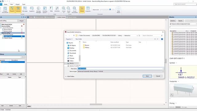
In part three of Learning SOLIDWORKS PCB we take a look at how to use PCB Libraries Solid Solutions is the leading SOLIDWORKS services provider delivering an expansive portfolio of solutions, ranging from 3D design (CAD), manufacturing (CAM) and data management (PDM/PLM) software tools, training, and technical support services, through to comprehensive business transformation programmes. Solid Solutions supports a community of more than 15,000 UK and Ireland-based customers, who encompass product designers, mechanical engineers, designers, manufacturers, and educational institutions across a wide range of industries. Need to find out more? Whether you're wondering where to start, looking to pick up some new tricks, or are just... Смотреть видео...
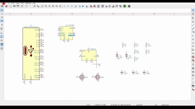
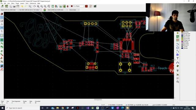
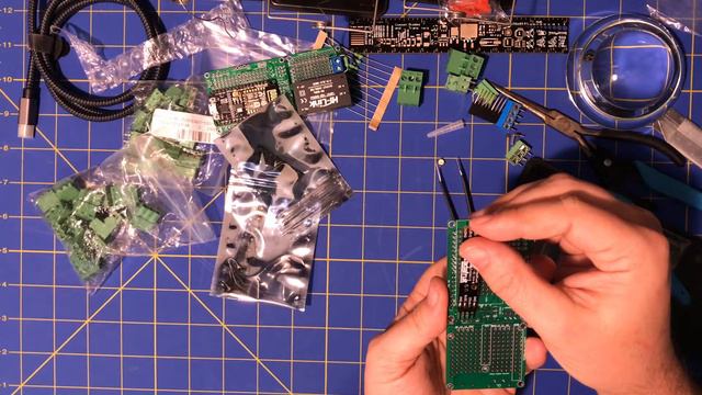
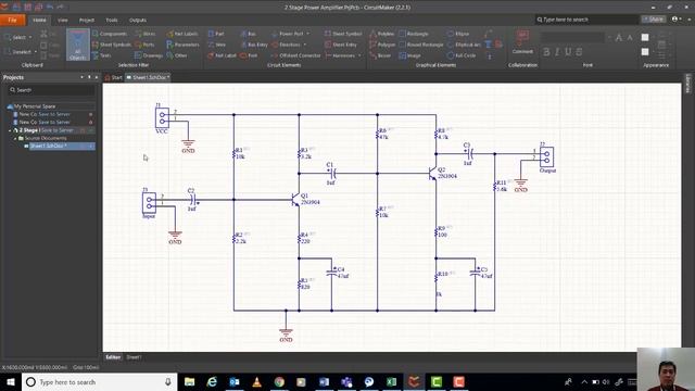
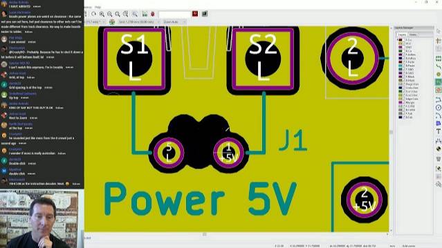
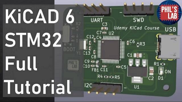
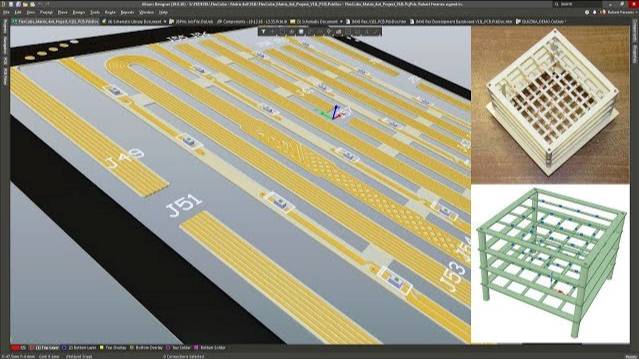
Complete step-by-step PCB design process going through the schematic, layout, and routing of a 'black-pill' STM32-based PCB including USB in the *new* KiCAD 6. All the way from schematic creation, through to two-layer PCB layout and routing, as well as sending it off for manufacture and assembly via JLCPCB. Mixed-signal hardware design course: [SUPPORT] Free trial of Altium Designer: PCBA from $0 (Free Setup, Free Stencil): Patreon: [LINKS] GitHub: [TIMESTAMPS] 00:00 Introduction 01:26 What You'll Learn (Schematic) 03:54 STM32 Microcontroller, Decoupling 15:01 STM32 Configuration Pins 21:15 Pin-Out and STM32CubeIDE 26:59 Crystal Circuitry 30:49 USB 33:57 Power Supply and Connectors 42:54 Electrical Rules Check (ERC),... Смотреть видео...
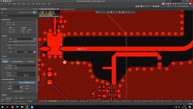
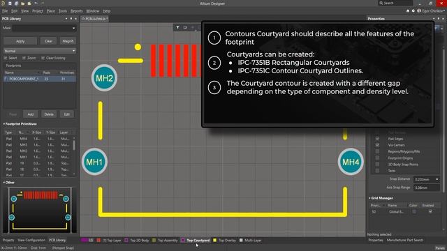
When working with PCB Design in Altium Designer, the courtyard is an essential piece. In this free Altium Designer training video, learn what a courtyard is, how to create it, and how to format a courtyard correctly for your PCB footprint. 0:00 What Is a PCB Footprint Courtyard? 0:24 What Should Courtyards Describe? 0:46 Courtyard Gap Values 1:21 How to Create Courtyards in Altium Designer For more PCB Layout videos, click here: For more Design Secrets: Creating a Footprint videos, click here: For more PCB Design for Beginners videos, click here: For more How To Use Altium Designer videos, click here: Design PCBs with a Free Trial of Altium Designer Here: Don't forget to follow us on social to stay up-to-date on the latest... Смотреть видео...
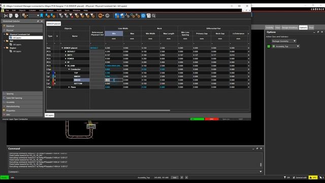
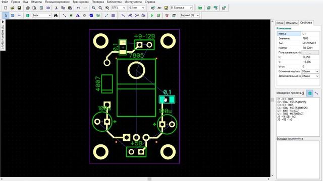
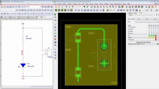
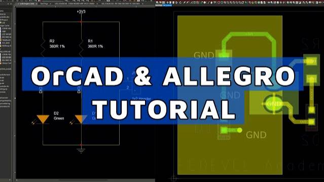
For everyone who would like to learn how to start with OrCad and Cadence Allegro. NEW: I updated this tutorial and here is the new version ( in case you need it ): Tutorial OrCAD 17.4 and Cadence Allegro PCB Editor | 2022 | Step by Step | For Beginners CHAPTERS: 00:00 - Introduction: What you are going to learn 02:35 - Starting a new project 03:56 - Creating Resistor Symbol 06:01 - Creating LED Symbol 08:35 - Creating Connector Symbol 09:19 - Creating Through hole pad 11:35 - Creating SMD pad 13:18 - Creating VIA 14:19 - Creating Resistor Footprint 16:12 - Creating Footprint for LED 17:31 - Creating Connector Footprint 18:54 - Assign footprints to symbols 19:57 - Placing components and Drawing Schematic 23:14 - Annotating... Смотреть видео...
After this tutorial you will know how to start designing your own boards in Cadence OrCAD and Allegro 17.4 . For everyone who would like to learn Allegro Design Entry CIS and Allegro PCB Editor and also for everyone who has never ever designed any boards, but would like to learn how to do it. Enjoy! Download the finished project here: Learn much more in our online courses here: In case you need a more detailed tutorial, this can help you: Chapters: 00:00 Introduction 00:34 What you will learn 01:33 *** Starting a new project *** 02:49 Creating a component in OrCAD - Header 04:17 Drawing a schematic symbol in OrCAD 05:52 Adding Part number property to symbol 06:50 Creating resistor schematic symbol 10:14 Creating LED schematic... Смотреть видео...
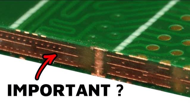
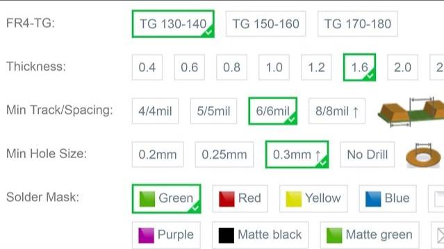
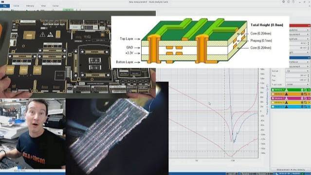
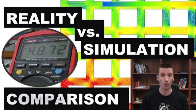
Are power planes in a 4 layer PCB any good as a capacitor? Can it work as one big bypass capacitor? A look at an discussion on PCB layer stackups, and some measurements on 4 and 8 layer PCB power planes with different prepreg thicknesses and how well they work as a capacitor. Forum: EEVblog Main Web Site: The 2nd EEVblog Channel: Support the EEVblog through Patreon! Stuff I recommend: Donate With Bitcoin & Other Crypto Currencies! T-Shirts: Likecoin – Coins for Likes: 💗 Likecoin – Coins for Likes: Теги: eevblog,video,pcb power plane,pcb design,pcb layout,pcb bypassing,power supply bypassing,bypass capacitor,frequency response,bode 100,capacitor resonance,pcb stackup,pcb prepreg,pcb prepreg material,fr4 fiberglass,fr4... Смотреть видео...
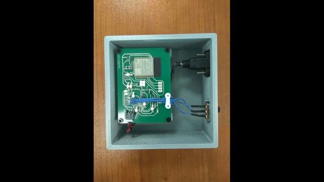
Σχεδίαση και κατασκευή πλακέτας με χρήση του Voltera V One Desktop PCB Printe. Design and assembly pcb board with Voltera V One Desktop PCB Printer. Στα πλαίσια εργασίας μου στο Ινστιτούτο Τεχνολογιών Πληροφορικής και Επικοινωνιών. #voltera #pcb #milling #assembly #electronics #certh #eketa #technology #soldering #smd #technology #soldering #smd #esp32 #rgb #led #resistors #capacitors #jumbers #cnc #milling #pcbassembly #pcbdesign #kicad #arduino #engineering #pcbassembly #raspberrypi #esp #technology #led #printedcircuitboard #electricalengineering #diyelectronics #electronicsengineering #microcontroller #robotics #altium #iot #embedded #circuit #pcbdesigner #electronicengineering #pcba #arduinoproject #pcbmanufacturing... Смотреть видео...
Dave answers a viewer technical question about why his circuit is acting up, and goes through a design review outlining the possible problems. Level translation, clocking, schmitt triggers, line driving, loading, buffering, bypassing, and other aspects are discussed. If you want to see more design reviews like this please drop a like and comment. Schitt Trigger Tutorial: Forum: Subscribe on Library: htts://lbry.tv/@eevblog:7 EEVblog Web Site: The 2nd EEVblog Channel: EEVdiscover: Support the EEVblog through Patreon! AliExpress Affiliate: Buy anything through that link and Dave gets a commission at no cost to you. Donate With Bitcoin & Other Crypto Currencies! T-Shirts: Теги: eevblog,video,design review,circuit design,pcb... Смотреть видео...
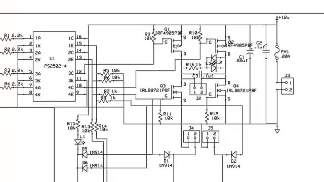
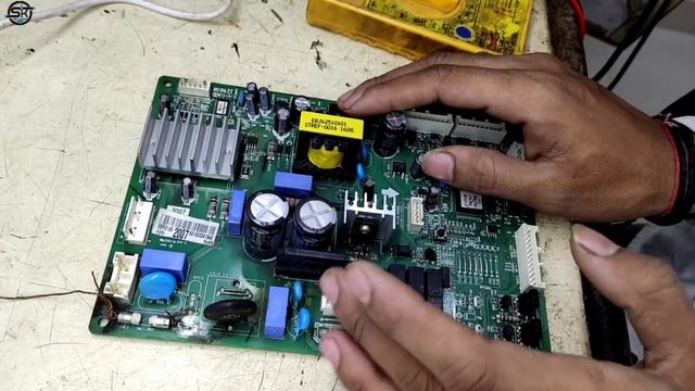
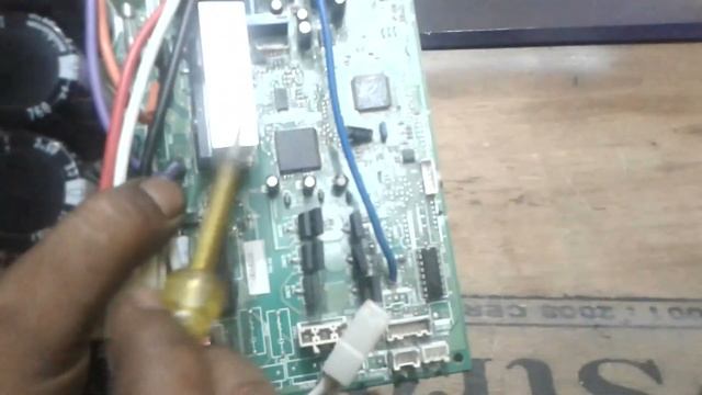
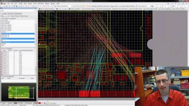
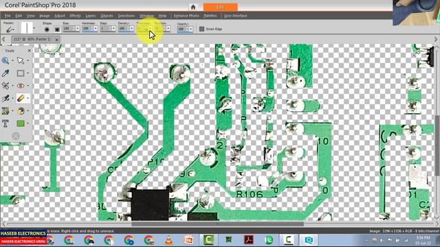
How To Draw Circuit Diagram From PCB / PCB Layout part-2. Reverse engineering technique for a furnished pcb. if circuit diagram / schematic / service manual is not available. so using how to reverse engineer a circuit board, i shared a very effective and simple technique. using this method, we get a picture from pcb using a photostat, scanner or getting a best resolution picture and we can get its print out. using pixlr online picture editing site and corel paintshop pro 2018, i erased the background between traces and finally placed component symbols on the diagram. then we can redraw the schematic / diagram. and putting components values, it becomes a perfect circuit diagram. You are Invited to Join Haseeb Electronics #howtodraw... Смотреть видео...
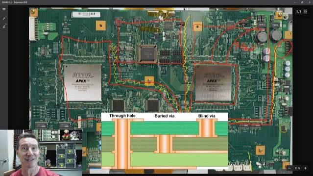
Only Dave can turn a simple question into a 1hr deep dive monologue into PCB layout and FPGA implementation. FPGA power supplies, DC margins, dynamic power requirements, power budgets, high power designs, multi layer PCB design, placement, system considerations, power planes, copper weighting, stackups, routing, split planes, star grounding, blind and buried vias, high speed traces, return paths, EMC, and a whole lot more. BGA Fanout Tutorial: IBM T221 Monitor Teardown: Bypass Capacitors Visualised: Forum: #FPGA #PCB #Design Bitcoin Donations: 38y7DE8HEHNj8fGDtUr4PkCn9nWxiorvvy Litecoin: ML7oQokTwB38bgzzjLDbRV97HKAHuwRfHA Ethereum: 0x11AceA38DCA9DbFfB4F35f3F746af65F9dED28ce EEVblog Main Web Site: The 2nd EEVblog Channel:... Смотреть видео...
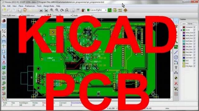
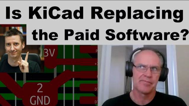
Is KiCad going to be always free? Is it now good enough to design any board? Who decides what new features will be implemented and where the project goes? Thank you Wayne for a great call. PS: Leave your comments, what do you think about KiCad and its future? Links: - Wayne Stambaugh: - KiCad: ------------------------------------------------------ Would you like to support me in what I do? It's simple: - you will help me a LOT, when you sign up for one of our Schematic and PCB Design online courses at The other ways to support me in what I do are: - Subscribe to this channel - support me through Patreon page - sign up for my Udemy course, Learn to Design Your Own Boards - send me an email and/or leave a positive comment - watch... Смотреть видео...
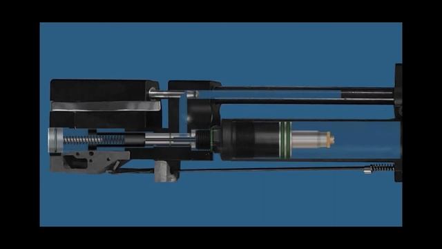
Я не разбираюсь в пневматических винтовках PCP от слова СОВСЕМ. Но я хочу показать, как бы я выбирал себе ПСП винтовку. ► Приветствую всех на канале НАШ ОПЫТ На своем опыте мы расскажем о различных домашних увлечениях и хобби. Тут будут как мужские хобби, так и хобби для женщин. Каждый сможет подобрать свое любимое хобби. Мы проведем с вами уютное время на нашей даче, покажем вам наш дачный загородный дом. Хоть это у нас всего лишь летняя дача и находиться она в Московской области, но пока нет своего загородного дома можно и тут проводить приятно время. Живем мы в городе Павловский Посад Московской области. Мы постараемся показать историю нашего города, проедем с вами по его старинным улицам и увидим, как изменился Павловский Посад за... Смотреть видео...
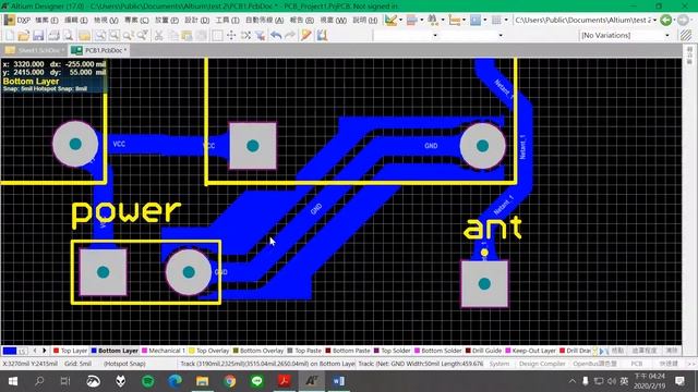
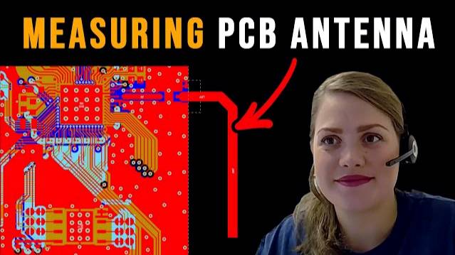
If you have a PCB antenna on your board, you need to know this. Thank you very much Kaja Sørbotten from Nordic Semiconductor. Links: - Kaja's LinkedIn: - Nordic Semiconductor: - FEDEVEL courses: Chapters: 00:00 What this video is about 03:53 Starting PCB antenna design (example nRF5340) 09:18 Where to get information about antenna dimensions 11:59 Antenna components and connection 18:24 Antenna and component placement 22:29 What is important in antenna PCB layout 27:18 AppCAD calculator 31:41 Common mistakes in PCB antenna designs 39:27 Measuring antenna output from the chip 43:20 Carrier frequency adjustment 50:58 Measuring output power and harmonics 59:10 Antenna output with matching components populated 1:02:47 Matching the antenna... Смотреть видео...
Change the way how you look at powers on your board. Part 2: PCB Layout & Decoupling - Understanding Impedance Part 3: PCB Layout & Decoupling - Measuring and Fixing Big THANK YOU to: - Florian Hämmerle - Eric Bogatin ------------------------------------------------------ Would you like to support me in what I do? It's simple: - you will help me a LOT, when you sign up for one of our Schematic and PCB Design online courses at The other ways to support me in what I do are: - Subscribe to this channel - support me through Patreon page - sign up for my Udemy course, Learn to Design Your Own Boards - send me an email and/or leave a positive comment - watch and like the videos :) - read my Welldone Blog at - spread a word about... Смотреть видео...
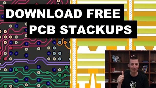
Stackups for you, so you have more time for doing PCB layout. Hope this helps. Links: - Share your PCB stackups here: - iMX6 Rex Module: - OpenRex: - Original post: CHAPTERS: 00:00 Intro 02:44 1. High Density Stackup 09:14 2. Motherboard Stackup 11:31 3. System on Module Stackup 15:32 4. SODIMM Computer on Module Stackup 18:53 5. Advanced Cost Effective Stackup 22:15 OpenRex Through hole 10 Layer stackup 25:00 Thank you ------------------------------------------------------ Would you like to support me in what I do? It's simple: - you will help me a LOT, when you sign up for one of our Schematic and PCB Design online courses at The other ways to support me in what I do are: - support me through Patreon page - sign up for my... Смотреть видео...