CAMTECH PCB-Mandy - видео - все видео
Новые видео из канала RuTube на сегодня - 20 April 2026 г.
Новые видео из канала RuTube на сегодня - 20 April 2026 г.
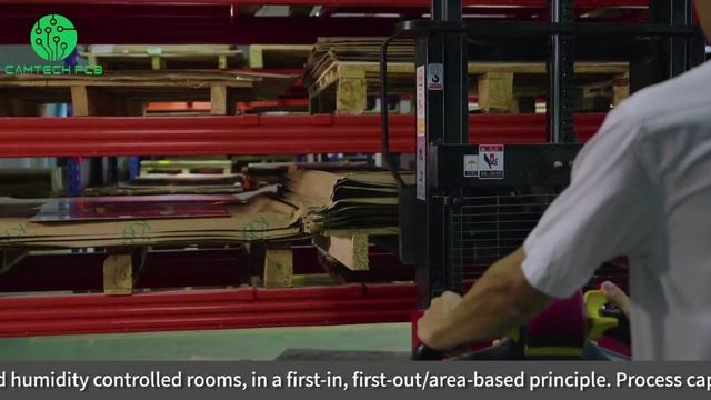
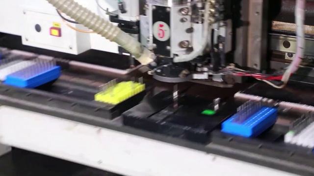
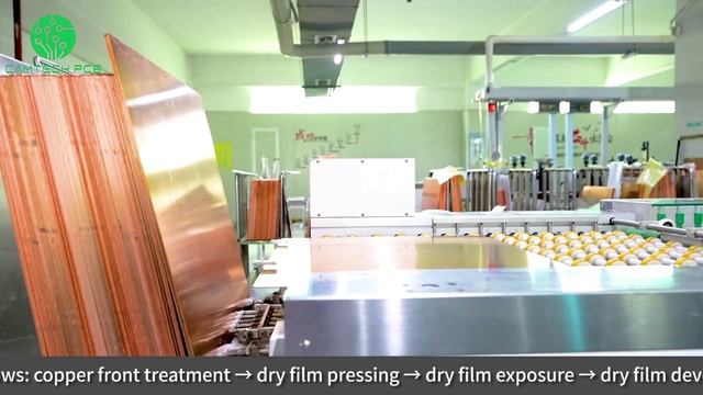
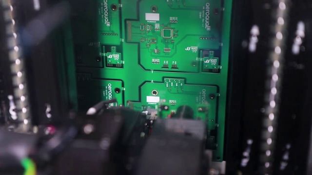
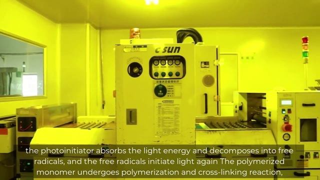
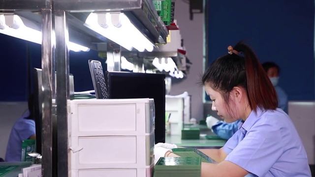
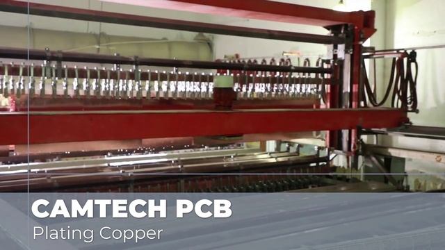
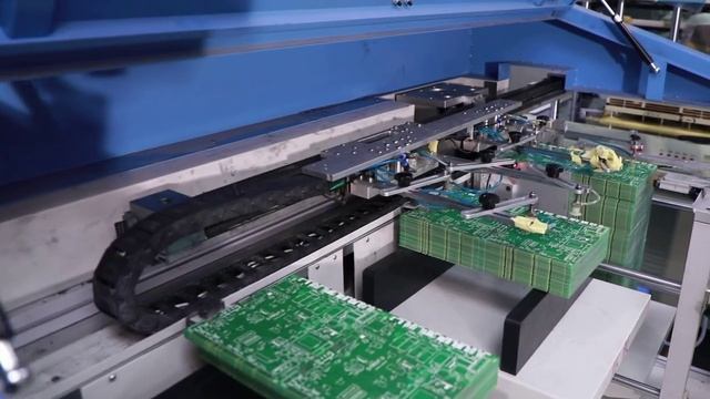
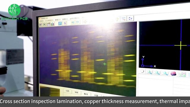
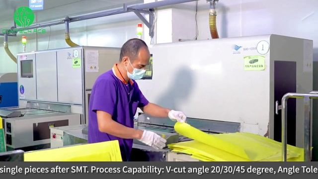
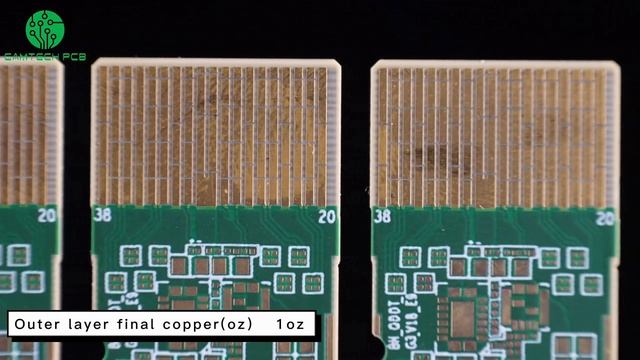
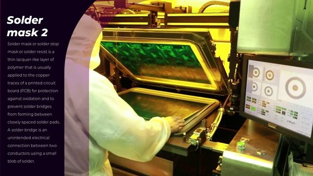
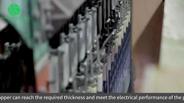
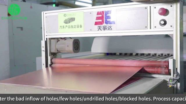
Material Warehouse (4 Floor). The design of takes into consideration many factors. They are good function and aesthetics, durability, economy, appropriated material, appropriated structure, personality/identity, etc. Website: www.camtechcircuits.com E-mail: sales03@camtechcircuits.comDrilling of PCB Board Drilling is to drill the required vias in the copper clad PCB board. PCB vias are divided into plated holes ( PTH ) and non-plated holes (NPTH) according to whether they are metallized. According to the process, it is divided into blind holes of the PCB, buried holes and through holes. Vias mainly provide electrical connections and are used for fixing or positioning devices. sales03@camtechcircuits.comVacuum Etching. Camtech PCB is a professional PCB manufacturer in China for 20 years. Website: www.camtechcircuits.com E-mail: sales03@camtechcircuits.comFlying Testing of PCB manufacturing The open circuit test principle of the flying probe test is the same as that of the needle bed test. Two probes are connected to the end of the network at the same time to energize, and the obtained resistance is compared with the set open circuit resistance to determine whether the open circuit is open or not. Flying probe test has the following advantages: Short test development cycle, Relatively low test cost, High conversion flexibility. Website: www.camtechcircuits.com E-mail: sales03@camtechcircuits.comThe purpose of the PCB circuit board exposure: through ultraviolet light irradiation and phenanthrene block for the PCB board. The transparent place of the film and the dry film undergo optical polymerization reaction, for the PCB manufacturing, that is, under ultraviolet light irradiation. The photoinitiator absorbs the light energy and decomposes into free radicals, and the free radicals initiate light again The polymerized monomer undergoes polymerization and cross-linking reaction, and forms a macromolecular structure insoluble in dilute alkali solution after the reaction. Website: www.camtechcircuits.com E-mail: sales03@camtechcircuits.comFinal Quality Inspection of PCB Zero defect is our goal,all our products,100% test and inspection, acceptance standard IPC-A-600-H and IPC-6012;100% Double Inspection before outgoing. Website: www.camtechcircuits.com Email: sales03@camtechcircuits.comPlating Copper of PCB manufacturing We have advanced copper plating line for PCB manufacturing, can ensure PCB copper thickness meet customer's requirement, the maximum copper thickness can reach inner layer 12 OZ, outer layer 12 OZ. Website: www.camtechcircuits.comE-Testing of Printed Circuit board The electronic test for PCB circuit boards is performed after manufactured. All the PCB must be checked with flying probe test. The layout is analysed according to the PCB file for short circuits and interruptions. This is important for PCB, because only the E-test detects incorrect and broken conductors. And the detected defective PCB circuit board will be rejected or marked. Website: www.camtechcircuits.com sales03@camtechcircuits.comAOI. The design of resorts to digital high tech. The foot types, arch types, foot type molding, and matching are collected and analyzed by the high tech.V-Cut. The quality of the product is maintained to meet the industry set norms and regulations by our strict quality management system.Solder mask 2 of PCB Solder mask or solder stop mask or solder resist is a thin lacquer-like layer of polymer that is usually applied to the copper traces of a printed circuit board (PCB) for protection against oxidation and to prevent solder bridges from forming between closely spaced solder pads. A solder bridge is an unintended electrical connection between two conductors using a small blob of solder. PCBs use solder masks to prevent this from happening. Solder mask is not always used for hand-soldered assemblies but is essential for mass-produced boards that are soldered automatically using reflow or Wave Solder techniques. Website: www.camtechcircuits.com